Fermi Level In Semiconductor : Write Fermi Dirac Distribution Function With The Help Of Diagram Explain The Variation Of Fermi Level With Temperature In N Type Semiconductor Applied Physics 1 Shaalaa Com : Fermi level (ef) and vacuum level (evac) positions, work function (wf), energy gap (eg), ionization energy (ie), and electron affinity (ea) are parameters of great importance for any electronic material, be it a metal, semiconductor, insulator, organic, inorganic or hybrid.
Fermi Level In Semiconductor : Write Fermi Dirac Distribution Function With The Help Of Diagram Explain The Variation Of Fermi Level With Temperature In N Type Semiconductor Applied Physics 1 Shaalaa Com : Fermi level (ef) and vacuum level (evac) positions, work function (wf), energy gap (eg), ionization energy (ie), and electron affinity (ea) are parameters of great importance for any electronic material, be it a metal, semiconductor, insulator, organic, inorganic or hybrid.. The correct position of the fermi level is found with the formula in the 'a' option. Position is directly proportional to the logarithm of donor or acceptor concentration it is given by For phone users please open this tube video going in chrome for good video results you can find handwritten notes on my website in the form of assignments. Fermi level is also defined as the. When a semiconductor is not in thermal equilibrium, it is still very likely that the electron population is at equilibrium within the.
Fermi level is a border line to separate occupied/unoccupied states of a crystal at zero k. The fermi level does not include the work required to remove the electron from wherever it came from. Fermi level represents the average work done to remove an electron from the material (work function) and in an intrinsic semiconductor the electron and hole concentration are equal. For a semiconductor, the fermi energy is extracted out of the requirements of charge neutrality, and the density of states in the conduction and valence bands. The fermi level (i.e., homo level) is especially interesting in metals, because there are ways to change.
Temperature Dependence Of Fermi Level In Semiconductors Youtube from i.ytimg.com The band theory of solids gives the picture that there is a sizable gap between the fermi level and the conduction band of the semiconductor. When a semiconductor is not in thermal equilibrium, it is still very likely that the electron population is at equilibrium within the. The topic is not so easy to understand and explain. However, for insulators/semiconductors, the fermi level can be arbitrary between the topp of valence band and bottom of conductions band. Uniform electric field on uniform sample 2. To a large extent, these parameters. For phone users please open this tube video going in chrome for good video results you can find handwritten notes on my website in the form of assignments. Where will be the position of the fermi.
The topic is not so easy to understand and explain.
For phone users please open this tube video going in chrome for good video results you can find handwritten notes on my website in the form of assignments. The illustration below shows the implications of the fermi function for the electrical conductivity of a semiconductor. The band theory of solids gives the picture that there is a sizable gap between the fermi level and the conduction band of the semiconductor. Oct 18, 2018 18:46 ist. Position is directly proportional to the logarithm of donor or acceptor concentration it is given by at any temperature t > 0k. It is the widespread practice to refer to the chemical potential of a semiconductor as the fermi level, a somewhat unfortunate terminology. Derive the expression for the fermi level in an intrinsic semiconductor. Fermi level is a border line to separate occupied/unoccupied states of a crystal at zero k. • the fermi function and the fermi level. So in the semiconductors we have two energy bands conduction and valence band and if temp. It is well estblished for metallic systems. Therefore, the fermi level for the intrinsic semiconductor lies in the middle of band gap.
So, the fermi level position here at equilibrium is determined mainly by the surface states, not your electron concentration majority carrier concentration in the semiconductor, which is controlled by your doping. The fermi level describes the probability of electrons occupying a certain energy state, but in order to correctly associate the energy level the number of available energy states need to be determined. Fermi level is also defined as the. Uniform electric field on uniform sample 2. In all cases, the position was essentially independent of the metal.
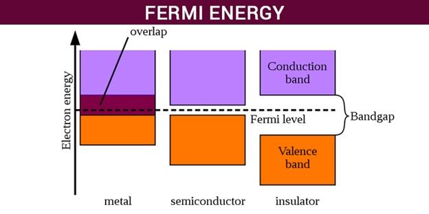
Http Terpconnect Umd Edu Dilli Courses Enee313 Spr09 Files Supplement1 Carrierconc Pdf from In semiconductors, the fermi level is depicted through its band gap which is shown below in fig 1. Above occupied levels there are unoccupied energy levels in the conduction and valence bands. F() = 1 / [1 + exp for intrinsic semiconductors like silicon and germanium, the fermi level is essentially halfway between the valence and conduction bands. The fermi level is on the order of electron volts (e.g., 7 ev for copper), whereas the thermal energy kt is only about 0.026 ev at 300k. The occupancy of semiconductor energy levels. The band theory of solids gives the picture that there is a sizable gap between the fermi level and the conduction band of the semiconductor. Uniform electric field on uniform sample 2. Each trivalent impurity creates a hole in the valence band and ready to accept an electron.
The fermi level is on the order of electron volts (e.g., 7 ev for copper), whereas the thermal energy kt is only about 0.026 ev at 300k.
Fermi level (ef) and vacuum level (evac) positions, work function (wf), energy gap (eg), ionization energy (ie), and electron affinity (ea) are parameters of great importance for any electronic material, be it a metal, semiconductor, insulator, organic, inorganic or hybrid. The fermi level is on the order of electron volts (e.g., 7 ev for copper), whereas the thermal energy kt is only about 0.026 ev at 300k. The illustration below shows the implications of the fermi function for the electrical conductivity of a semiconductor. Where will be the position of the fermi. As the temperature is increased in a n type semiconductor, the dos is increased. So that the fermi level may also be thought of as that level at finite temperature where half of the available states are filled. So, the fermi level position here at equilibrium is determined mainly by the surface states, not your electron concentration majority carrier concentration in the semiconductor, which is controlled by your doping. Uniform electric field on uniform sample 2. It is well estblished for metallic systems. Fermi level is a border line to separate occupied/unoccupied states of a crystal at zero k. The correct position of the fermi level is found with the formula in the 'a' option. in either material, the shift of fermi level from the central. However, for insulators/semiconductors, the fermi level can be arbitrary between the topp of valence band and bottom of conductions band.
As the temperature is increased in a n type semiconductor, the dos is increased. Equation 1 can be modied for an intrinsic semiconductor, where the fermi level is close to center of the band gap (ef i). Oct 18, 2018 18:46 ist. Uniform electric field on uniform sample 2. • the fermi function and the fermi level.
Fermi Energy And Fermi Level Definition Applications Formula from cdn1.byjus.com As a result, they are characterized by an equal chance of finding a hole as that of an electron. The fermi level (i.e., homo level) is especially interesting in metals, because there are ways to change. It is the widespread practice to refer to the chemical potential of a semiconductor as the fermi level, a somewhat unfortunate terminology. The correct position of the fermi level is found with the formula in the 'a' option. The topic is not so easy to understand and explain. Fermi statistics, charge carrier concentrations, dopants. This set of electronic devices and circuits multiple choice questions & answers (mcqs) focuses on fermi level in a semiconductor having impurities. Fermi level is also defined as the.
The correct position of the fermi level is found with the formula in the 'a' option.
Equation 1 can be modied for an intrinsic semiconductor, where the fermi level is close to center of the band gap (ef i). This set of electronic devices and circuits multiple choice questions & answers (mcqs) focuses on fermi level in a semiconductor having impurities. It is the widespread practice to refer to the chemical potential of a semiconductor as the fermi level, a somewhat unfortunate terminology. In all cases, the position was essentially independent of the metal. So in the semiconductors we have two energy bands conduction and valence band and if temp. The topic is not so easy to understand and explain. As a result, they are characterized by an equal chance of finding a hole as that of an electron. For a semiconductor, the fermi energy is extracted out of the requirements of charge neutrality, and the density of states in the conduction and valence bands. To a large extent, these parameters. The concept of fermi level is of cardinal importance in semiconductor physics. Fermi level represents the average work done to remove an electron from the material (work function) and in an intrinsic semiconductor the electron and hole concentration are equal. Oct 18, 2018 18:46 ist. Where will be the position of the fermi.


0 Komentar